NCP6361 Description
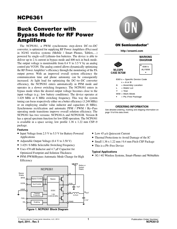
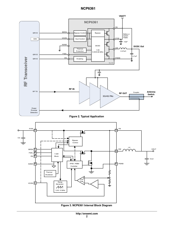
NCP6361 Buck Converter with Bypass Mode for RF Power Amplifiers The NCP6361, a PWM synchronous step−down DC−to−DC converter, is optimized for supplying RF Power Amplifiers (PAs) used in 3G/4G wireless systems (Mobile / Smart Phones, Tablets,…) powered by single−cell Lithium−Ion batteries. The device is able to deliver up to 2 A current in bypass mode and 800 mA in buck mode. The output voltage is monitorable from...
NCP6361 Key Features
- Input Voltage from 2.5 V to 5.5 V for Battery Powered
NCP6361 Applications
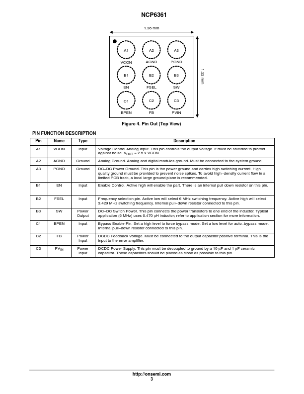
- Adjustable Output Voltage (0.4 V to 3.50 V)