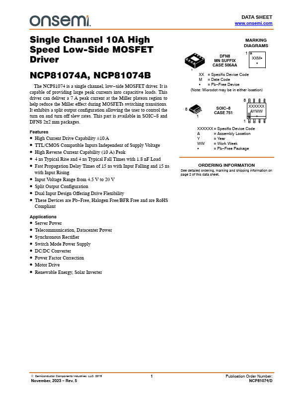
NCP81074A Overview
Key Features
- High Current Drive Capability ±10 A
- TTL/CMOS Compatible Inputs Independent of Supply Voltage
- High Reverse Current Capability (10 A) Peak
- 4 ns Typical Rise and 4 ns Typical Fall Times with 1.8 nF Load
- Fast Propagation Delay Times of 15 ns with Input Falling and 15 ns with Input Rising
- Input Voltage Range from 4.5 V to 20 V
- Split Output Configuration
- Dual Input Design Offering Drive Flexibility
- These Devices are Pb-Free, Halogen Free/BFR Free and are RoHS Compliant