NCV1124
NCV1124 is Dual Variable Reluctance Sensor Interface IC manufactured by onsemi.
Features
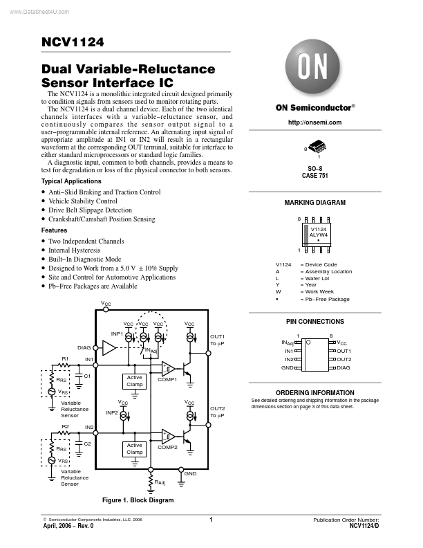
VCC VCC VCC INP1 DIAG R1 IN1 C1
+
- VCC OUT1 To m P
PIN CONNECTIONS
1 INAdj IN1 IN2 GND 8 VCC OUT1 OUT2 DIAG
INAdj
RRS VRS
Active Clamp VCC INP2
P1
ORDERING INFORMATION
VCC OUT2 To m P
+
- See detailed ordering and shipping information in the package dimensions section on page 3 of this data sheet.
Variable Reluctance Sensor R2 IN2 C2
RRS VRS
Active Clamp
P2
Variable Reluctance Sensor
GND RAdj
Figure 1. Block Diagram
© Semiconductor ponents Industries, LLC, 2006
April, 2006
- Rev. 0
Publication Order Number: NCV1124/D
MAXIMUM RATINGS
Rating Storage Temperature Range Ambient Operating Temperature Supply Voltage Range (continuous) Input Voltage Range (at any input, R1 = R2 = 22 k) Maximum Junction Temperature ESD Susceptibility (Human Body Model) Lead Temperature Soldering: Reflow: (SMD styles only) (Note 1) Value
- 65 to 150
- 40 to 125
- 0.3 to 7.0
- 250 to 250 150 2.0 240 peak Unit °C °C V V °C k V °C
Stresses exceeding Maximum Ratings may damage the device. Maximum Ratings are stress ratings only. Functional operation above the Remended Operating Conditions is not implied. Extended exposure to stresses above the Remended Operating Conditions may affect device reliability. 1. 60 second maximum above 183°C.
ELECTRICAL CHARACTERISTICS (4.5 V < VCC < 5.5 V,
- 40°C < TA < 125°C, VDIAG = 0; unless otherwise specified.)
Characteristic VCC SUPPLY Operating Current Supply Sensor Inputs Input Threshold
- Positive Input Threshold
- Negative Input Bias Current (INP1, INP2) Input Bias Current (DIAG) Input Bias Current Factor (KI) (INAdj = INP × KI) Bias Current Matching Input Clamp
- Negative Input Clamp
-...