NCV5701B
features include accurate Under- voltage- lockout (UVLO), desaturation protection (DESAT) and Active Low FAULT output. The drivers also feature an accurate 5.0 V output. The drivers are designed to acmodate a wide voltage range of bias supplies including unipolar and NCV5701B even bipolar voltages.
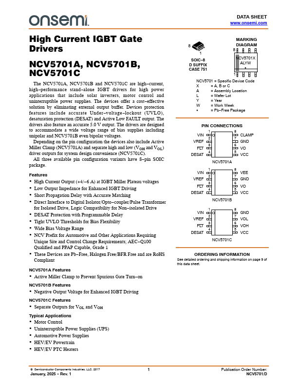
Depending on the pin configuration the devices also include Active Miller Clamp (NCV5701A) and separate high and low (VOH and VOL) driver outputs for system design convenience (NCV5701C).
All three available pin configuration variants have 8- pin SOIC package.
Features
- High Current Output (+4/- 6 A) at IGBT Miller Plateau voltages
- Low Output Impedance for Enhanced IGBT Driving
- Short Propagation Delay with Accurate Matching
- Direct Interface to Digital Isolator/Opto- coupler/Pulse Transformer for Isolated Drive, Logic patibility for Non- isolated Drive
- DESAT Protection with Programmable Delay
- Tight UVLO Thresholds for Bias Flexibility
- Wide Bias Voltage Range
- NCV Prefix for...