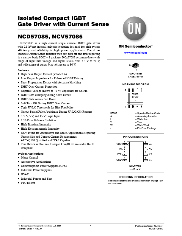
NCV57085
Overview
- High Peak Output Current (+7A/-7 A)
- Low Output Impedance for Enhanced IGBT Driving
- Short Propagation Delays with Accurate Matching
- IGBT Over Current Protection
- Negative Voltage (Down to -9 V) Capability for CS Pin
- IGBT Gate Clamping during Short Circuit
- IGBT Gate Active Pull Down
- Soft Turn Off During IGBT Over Current
- Tight UVLO Thresholds for Bias Flexibility
- Output Partial Pulse Avoidance During UVLO/CS (Restart)