NIS6201
NIS6201 is Regulated Charge Pump manufactured by onsemi.
Floating, Regulated Charge Pump
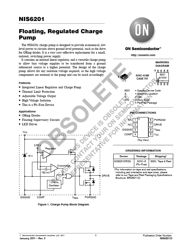
The NIS6201 charge pump is designed to provide economical, low level power to circuits above ground level potential, such as the drive for ORing diodes. It is a very cost- effective replacement for a small, isolated, switching power supply.
It contains an internal linear regulator, and a versatile charge pump to allow bias voltage supplies to be transferred from a ground referenced source to a higher potential. The design of the charge pump allows for any isolation voltage required, as the high voltage ponents are external to the pump and can be sized accordingly.
Features
- Integrated Linear Regulator and Charge Pump
- Thermal Limit Protection
-...