NL17SG00 Overview
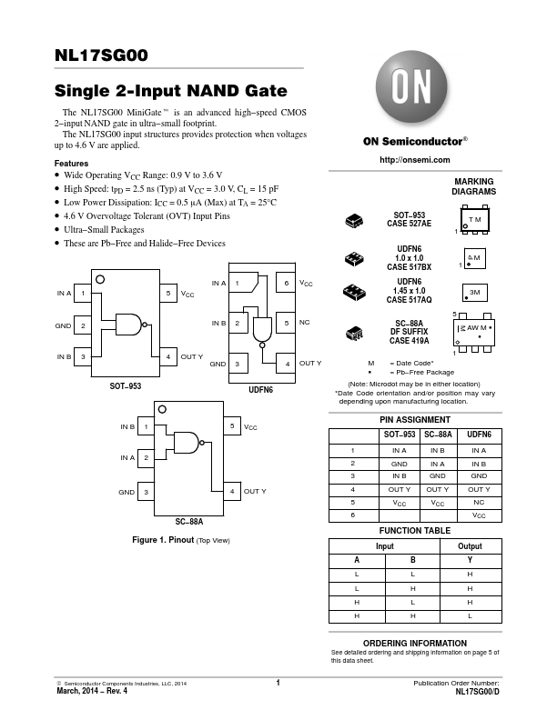
Key Features
- Wide Operating VCC Range: 0.9 V to 3.6 V
- High Speed: tPD = 2.5 ns (Typ) at VCC = 3.0 V, CL = 15 pF
- Low Power Dissipation: ICC = 0.5 mA (Max) at TA = 25°C
- 4.6 V Overvoltage Tolerant (OVT) Input Pins
- Ultra-Small Packages
| Part | NL17SG00 |
|---|---|
| Description | Single 2-Input NAND Gate |
| Manufacturer | onsemi |
| Size | 103.93 KB |
| Part Number | Manufacturer | Description |
|---|---|---|
| NSi6602 | NOVOSENSE | High Reliability Isolated Dual-Channel Gate Driver |
| NSi6801 | NOVOSENSE | Single-Channel Isolated Gate Driver |
| FD2103 | Fortior | 180V Half-Bridge Gate Driver |