Datasheet4U Logo Datasheet4U.com

NL17SHT126 - Noninverting Buffer / CMOS Logic Level Shifter

Features

  • High Speed: tPD = 3.5 ns (Typ) at VCC = 5 V.
  • Low Power Dissipation: ICC = 1 mA (Max) at TA = 25°C.
  • TTL.
  • Compatible Inputs: VIL = 0.8 V; VIH = 2 V.
  • CMOS.
  • Compatible Outputs: VOH > 0.8 VCC; VOL < 0.1 VCC @Load.
  • Power Down Protection Provided on Inputs and Outputs.
  • Balanced Propagation Delays.
  • Pin and Function Compatible with Other Standard Logic Families.
  • These are Pb.
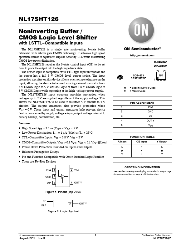
  • Free Devices IN A 1 GND 2 OE 3 5 V.

📥 Download Datasheet

Datasheet preview – NL17SHT126

Datasheet Details

Part number NL17SHT126
Manufacturer onsemi
File Size 128.11 KB
Description Noninverting Buffer / CMOS Logic Level Shifter
Datasheet download datasheet NL17SHT126 Datasheet
Additional preview pages of the NL17SHT126 datasheet.
Other Datasheets by ON Semiconductor

Full PDF Text Transcription

Click to expand full text
NL17SHT126 Noninverting Buffer / CMOS Logic Level Shifter with LSTTL−Compatible Inputs The NL17SHT126 is a single gate noninverting 3−state buffer fabricated with silicon gate CMOS technology. It achieves high speed operation similar to equivalent Bipolar Schottky TTL while maintaining CMOS low power dissipation. The NL17SHT126 requires the 3−state control input (OE) to be set Low to place the output into the high impedance state. The device input is compatible with TTL−type input thresholds and the output has a full 5 V CMOS level output swing. The input protection circuitry on this device allows overvoltage tolerance on the input, allowing the device to be used as a logic−level translator from 3 V CMOS logic to 5 V CMOS Logic or from 1.
Published: |