NL17SV02XV5T2
NL17SV02XV5T2 is Single 2-Input NOR Gate manufactured by onsemi.
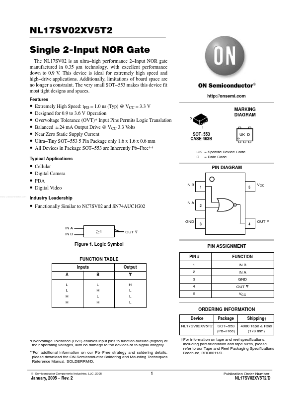
Features http://onsemi. MARKING DIAGRAM
1 SOT- 553 CASE 463B UK D
- -
- -
- -
- -
- -
- ..
Extremely High Speed: t PD = 1.0 ns (Typ) @ VCC = 3.3 V Designed for 0.9 to 3.6 V Operation Overvoltage Tolerance (OVT)- Input Pins Permits Logic Translation Balanced "24 m A Output Drive @ VCC 3.3 Volts Near Zero Static Supply Current Ultra- Tiny SOT- 553 5 Pin Package only 1.6 x 1.6 x 0.6 mm All Devices in Package SOT- 553 are Inherently Pb- Free-
- 5
Typical Applications
UK = Specific Device Code D = Date Code
Cellular Digital Camera PDA Digital Video
PIN DIAGRAM
IN B
Industry Leadership
- Functionally Similar to NC7SV02 and SN74AUC1G02
IN A
GND IN A IN B 1 OUT Y
OUT Y
Figure 1. Logic Symbol FUNCTION TABLE
Inputs A L L H H B L H L H Output Y H L L L PIN # 1 2 3 4 5
PIN ASSIGNMENT
FUNCTION IN B IN A GND OUT Y VCC
ORDERING INFORMATION
Device NL17SV02XV5T2 Package SOT- 553 (Pb- Free) Shipping† 4000 Tape & Reel (178 mm)
- Overvoltage Tolerance (OVT) enables input pins to function outside (higher) of their operating voltages, with no damage to the devices or to signal integrity.
- - For additional information on our Pb- Free strategy and soldering details, please download the ON Semiconductor Soldering and Mounting Techniques Reference Manual, SOLDERRM/D.
© Semiconductor ponents Industries, LLC, 2005
†For information on tape and reel specifications, including part orientation and tape sizes, please refer to our Tape and Reel Packaging Specifications Brochure, BRD8011/D.
January, 2005
- Rev. 2
Publication Order Number: NL17SV02XV5T2/D
MAXIMUM RATINGS
Symbol VCC VI VO IIK IOK IO ICC IGND TSTG TL TJ q JA PD MSL FR VESD DC Supply Voltage DC Input Voltage DC Output Voltage DC Input Diode Current DC Output Diode Current DC Output Sink Current DC Supply Current per Supply Pin DC Ground Current per Ground Pin Storage Temperature Range Lead Temperature, 1.0 mm from Case for 10 seconds Junction Temperature Under Bias Thermal Resistance (Note 1)...