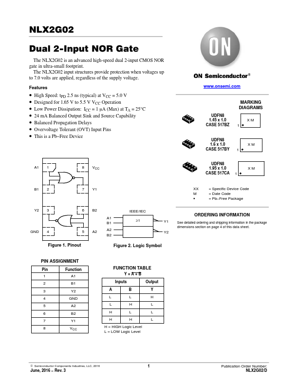
NLX2G02 Key Features
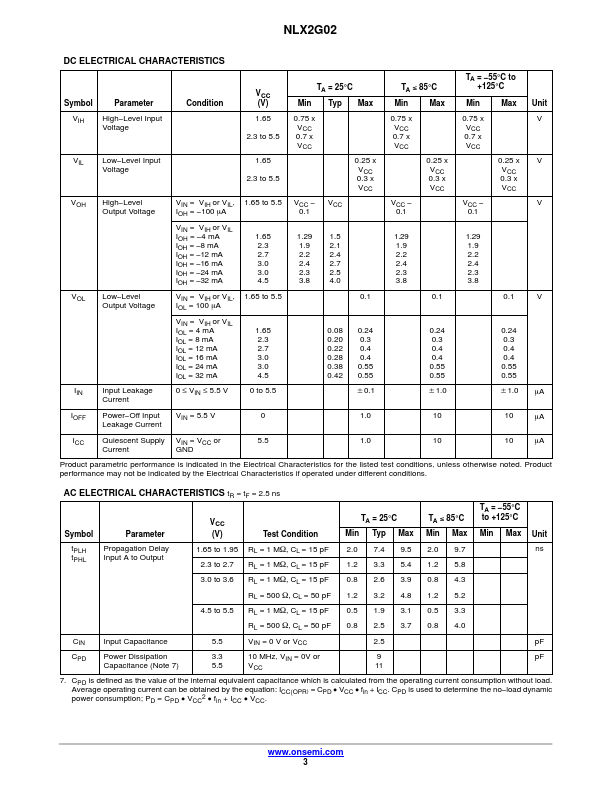
- High Speed: tPD 2.5 ns (typical) at VCC = 5.0 V
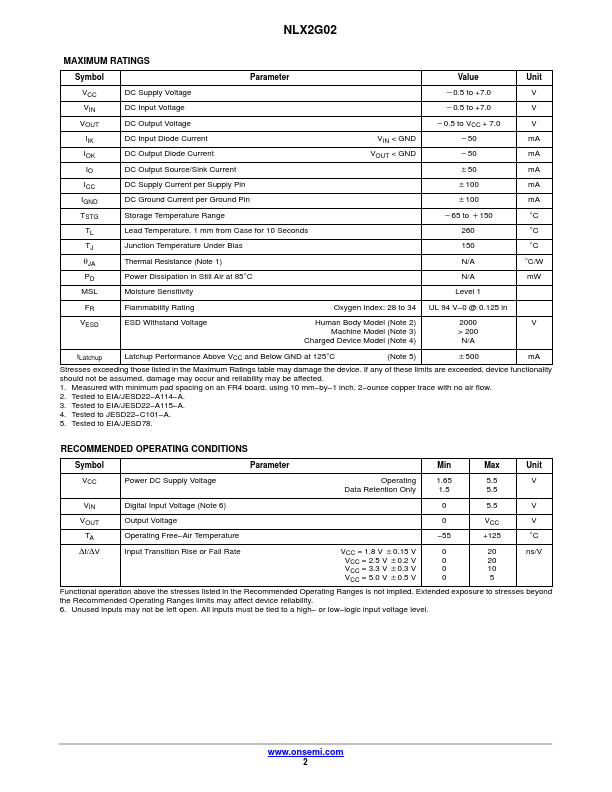
- Designed for 1.65 V to 5.5 V VCC Operation
- Low Power Dissipation: ICC = 1 mA (Max) at TA = 25°C
- 24 mA Balanced Output Sink and Source Capability
- Balanced Propagation Delays
- Overvoltage Tolerant (OVT) Input Pins
- This is a Pb-Free Device
- Rev. 3