NSVBSS63LT1G Description
High Voltage Transistor PNP Silicon BSS63LT1G, NSVBSS63LT1G.
NSVBSS63LT1G Key Features
- NSV Prefix for Automotive and Other
NSVBSS63LT1G is PNP Silicon High Voltage Transistor manufactured by onsemi .
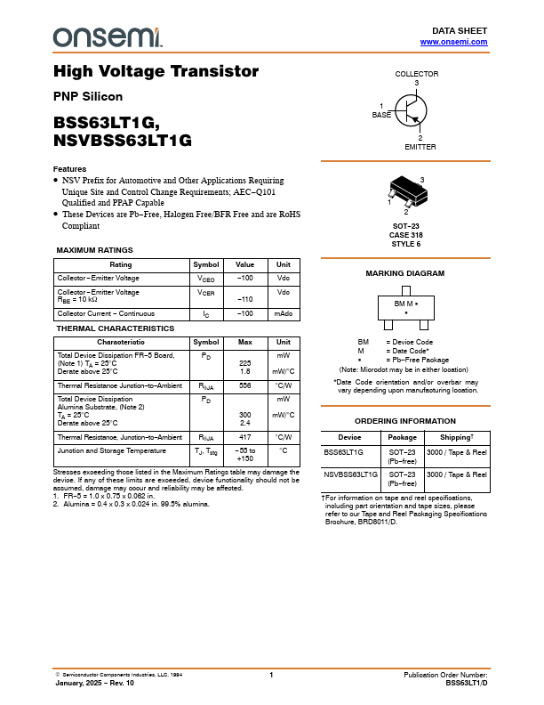
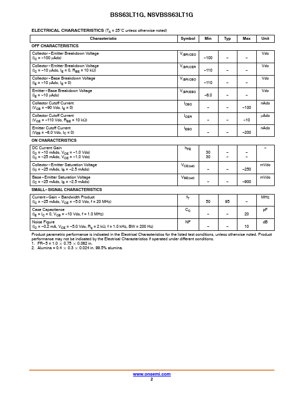
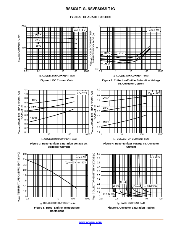
High Voltage Transistor PNP Silicon BSS63LT1G, NSVBSS63LT1G.