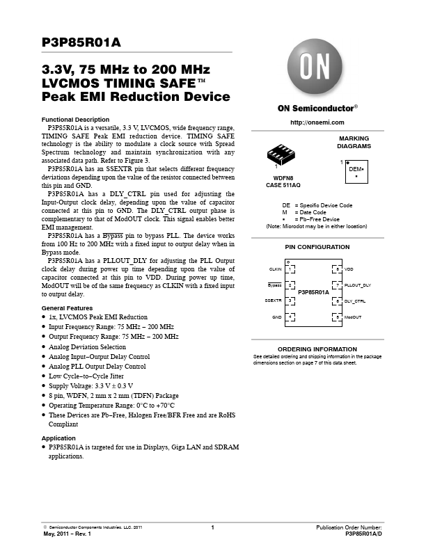
P3P85R01A Description
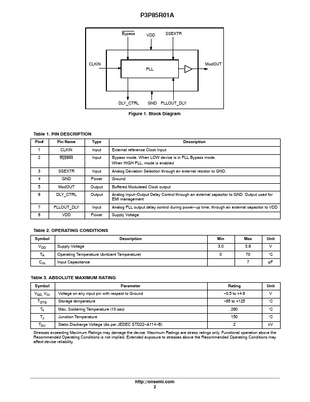
P3P85R01A is a versatile, 3.3 V, LVCMOS, wide frequency range, TIMING SAFE Peak EMI reduction device. TIMING SAFE technology is the ability to modulate a clock source with Spread Spectrum technology and maintain synchronization with any associated data path. P3P85R01A has an SSEXTR pin that selects different frequency deviations depending upon the value of the resistor connected between this pin and GND.
P3P85R01A Key Features
- 1x, LVCMOS Peak EMI Reduction
- Input Frequency Range: 75 MHz
- 200 MHz
- Output Frequency Range: 75 MHz
- 200 MHz
- Analog Deviation Selection
- Analog Input-Output Delay Control
- Analog PLL Output Delay Control
- Low Cycle-to-Cycle Jitter
- Supply Voltage: 3.3 V ± 0.3 V