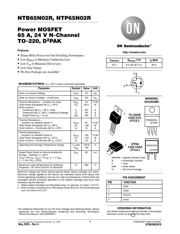
P65N02RG
Features
- Planar HD3e Process for Fast Switching Performance
- Low RDSon to Minimize Conduction Loss
- Low Ciss to Minimize Driver Loss
- Low Gate Charge
- Pb- Free Packages are Available- http://onsemi.
V(BR)DSS 24 V
RDS(on) TYP 8.4 m W @ 10 V
ID MAX 65 A
MAXIMUM RATINGS (TJ = 25°C Unless otherwise specified)
Parameter
Symbol Value Unit
Drain- to- Source Voltage
Gate- to- Source Voltage
- Continuous
Thermal Resistance
- Junction- to- Case Total Power Dissipation @ TC = 25°C Drain Current
- Continuous @ TC = 25°C, Chip Continuous @ TC =25°C, Limited by Package Single Pulse (tp = 10 ms)
VDSS
Rq JC PD
ID ID IDM
±20
2.0 62.5
Vdc
Vdc
°C/W W
160 A
Thermal Resistance
- Junction- to- Ambient (Note 1)
Total Power Dissipation @ TA = 25°C Drain Current
- Continuous @ TA = 25°C
Thermal Resistance
- Junction- to- Ambient (Note 2)
Total Power Dissipation @ TA = 25°C Drain Current
- Continuous @ TA = 25°C
Operating and Storage Temperature...