Protection diode in
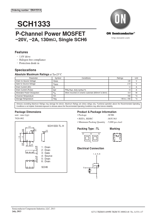
Specifications
Absolute Maximum Ratings at Ta=25°C
Parameter
Symbol
Drain-to-Source Voltage Gate-to-Source Voltage Drain Current (DC) Drain Current (Pulse) Allowable Power Dissipation Channel Temperature
VDSS VGSS ID IDP PD Tch
Storage Temperature
Tstg
Conditions
PW≤10μs, duty cycle≤1% When mounted on ceramic substrate (900mm2×0.8mm)
Ratings --20 ±10 --2 --8 0.8 150
--55 to +150
Unit V V A A W °C °C
S.
Full PDF Text Transcription for SCH1333 (Reference)
Note: Below is a high-fidelity text extraction (approx. 800 characters) for
SCH1333. For precise diagrams, and layout, please refer to the original PDF.
Ordering number : ENA1531A SCH1333 P-Channel Power MOSFET –20V, –2A, 130mΩ, Single SCH6 http://onsemi.com Features • 1.8V drive • Halogen free compliance • Protection dio...
View more extracted text
i.com Features • 1.8V drive • Halogen free compliance • Protection diode in Specifications Absolute Maximum Ratings at Ta=25°C Parameter Symbol Drain-to-Source Voltage Gate-to-Source Voltage Drain Current (DC) Drain Current (Pulse) Allowable Power Dissipation Channel Temperature VDSS VGSS ID IDP PD Tch Storage Temperature Tstg Conditions PW≤10μs, duty cycle≤1% When mounted on ceramic substrate (900mm2×0.8mm) Ratings --20 ±10 --2 --8 0.8 150 --55 to +150 Unit V V A A W °C °C Stresses exceeding Maximum Ratings may damage the device. Maximum Ratings are stress ratings only. Functional operation above the Recommended Operating
 SCH1333 Datasheet