Datasheet4U Logo Datasheet4U.com

SFT1350 - P-Channel Power MOSFET

Key Features

  • ON-resistance RDS(on)1=45mΩ(typ. ).
  • Input Capacitance Ciss=590pF(typ. ).
  • Halogen free compliance.
  • Protection diode in.
  • 4.5V drive Specifications Absolute Maximum Ratings at Ta=25°C Parameter Symbol Drain-to-Source Voltage Gate-to-Source Voltage Drain Current (DC) Drain Current (PW≤10μs) VDSS VGSS ID IDP Allowable Power Dissipation PD Channel Temperature Storage Temperature Tch Tstg Conditions PW≤10μs, duty cycle≤1% Tc=25°C Ratings --40 ±.

📥 Download Datasheet

Datasheet Details

Part number SFT1350
Manufacturer onsemi
File Size 314.65 KB
Description P-Channel Power MOSFET
Datasheet download datasheet SFT1350 Datasheet

Full PDF Text Transcription (Reference)

The following content is an automatically extracted verbatim text from the original manufacturer datasheet and is provided for reference purposes only.

View original datasheet text
Ordering number : 
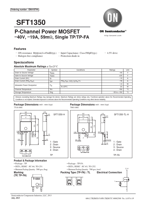
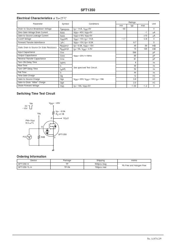
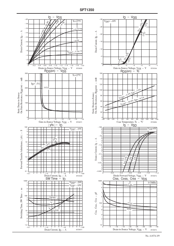
ENA1874A SFT1350 P-Channel Power MOSFET –40V, –19A, 59mΩ, Single TP/TP-FA http://onsemi.com Features • ON-resistance RDS(on)1=45mΩ(typ.) • Input Capacitance Ciss=590pF(typ.) • Halogen free compliance • Protection diode in • 4.5V drive Specifications Absolute Maximum Ratings at Ta=25°C Parameter Symbol Drain-to-Source Voltage Gate-to-Source Voltage Drain Current (DC) Drain Current (PW≤10μs) VDSS VGSS ID IDP Allowable Power Dissipation PD Channel Temperature Storage Temperature Tch Tstg Conditions PW≤10μs, duty cycle≤1% Tc=25°C Ratings --40 ±20 --19 --76 1.0 23 150 --55 to +150 Unit V V A A W W °C °C Stresses exceeding Maximum Ratings may damage the device. Maximum Ratings are stress ratings only.