Full PDF Text Transcription for TND322VD (Reference)
Note: Below is a high-fidelity text extraction (approx. 800 characters) for
TND322VD. For precise diagrams, and layout, please refer to the original PDF.
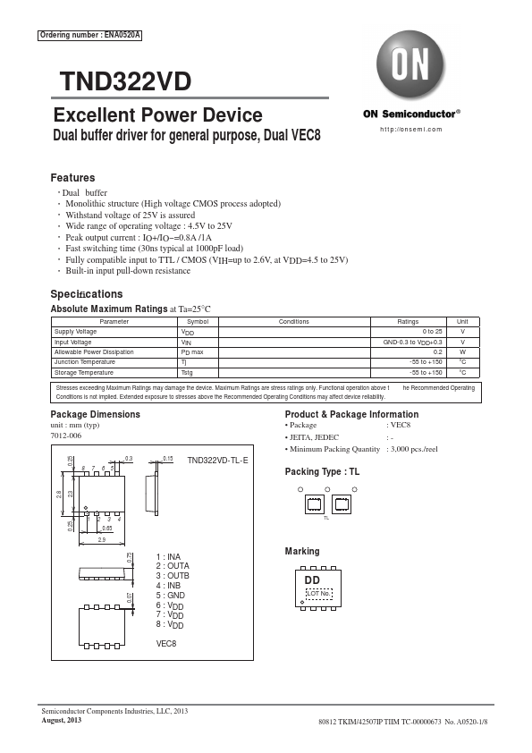
Ordering number : ENA0520A TND322VD Excellent Power Device Dual buffer driver for general purpose, Dual VEC8 Features Dual buffer Monolithic structure (High voltage CMOS ...
View more extracted text
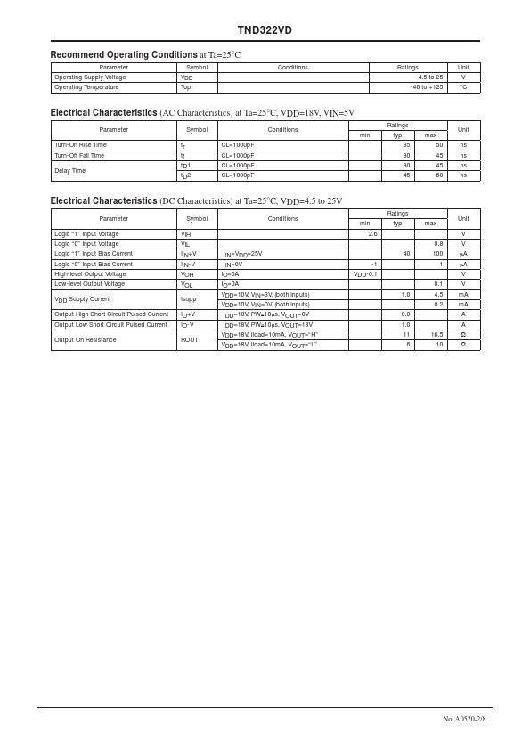
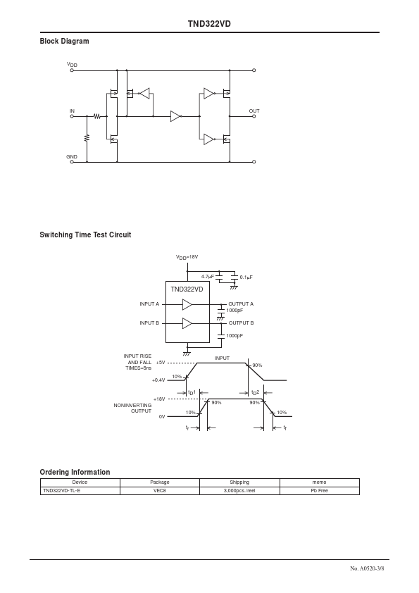
ual VEC8 Features Dual buffer Monolithic structure (High voltage CMOS process adopted) • Withstand voltage of 25V is assured • Wide range of operating voltage : 4.5V to 25V • Peak output current : IO+/IO--=0.8A /1A • Fast switching time (30ns typical at 1000pF load) • Fully compatible input to TTL / CMOS (VIH=up to 2.6V, at VDD=4.5 to 25V) • Built-in input pull-down resistance • • http://onsemi.com Specifications Absolute Maximum Ratings at Ta=25°C Parameter Supply Voltage Input Voltage Allowable Power Dissipation Junction Temperature Storage Temperature Symbol VDD VIN PD max Tj Tstg Conditions Ratings 0 to 25 GND-0.3 to VD
 TND322VD Datasheet