FEATURES
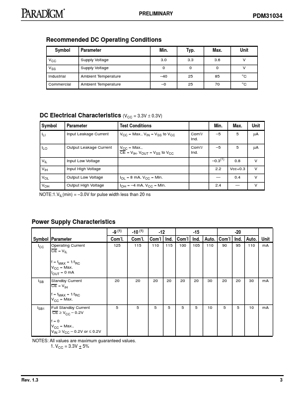
n High-speed access times Com’l: 9, 10, 12, 15 and 20 ns Ind’l.: 12, 15 and 20 ns Automotive: 15 and 20 ns n Low power operation (typical) - PDM31034SA Active: 200 mW Standby: 15 mW n Single +3.3V (±0.3V) power supply n TTL-compatible inputs and outputs n Packages Plastic SOJ (400 mil) - SO Plastic SOJ (300 mil) - TSO Plastic TSOP (II) - T PRELIMINARY PDM31034 1 Megabit 3.3V Static RAM 1 128K x 8-Bit Revolutionary Pinout DESCRIPTION
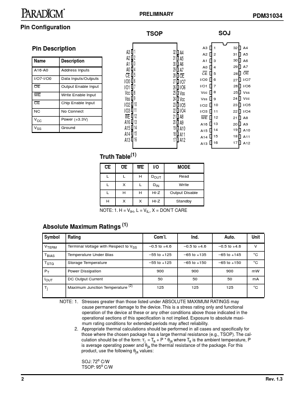
2 Writing is accomplished when the write enable (WE) and the chip enable (CE) inputs are both LOW. Reading is 3 accomplished when WE remains HIGH and CE and OE are both LOW. 5 6 Functional Block Diagram Addresses A8 Row Address Buffer Row Decoder A0 Memory Array 512 x 256 x 8 (1,048,576) I/O0 Input Data Control Column I/O Column Decoder I/O7 Column Address Buffer CE Control WE OE A16 A9 7 8 9 10 11 12 Rev. 1.3 1 Pin Configuration PRELIMINARY TSOP SOJ PDM31034 Pin DESCRIPTION
Name A16-A0 I/O7-I/O0 OE WE CE NC VCC VSS DESCRIPTION
Address Inputs Data I...