P10V50SP
P10V50SP is MOS Schottky Rectifier manufactured by PFC Device Corporation.
Features
- Ultra Low Forward Voltage Drop
- Reliable High Temperature Operation
- Softest, fast switching capability
- 150o C Operating Junction Temperature
- Lead Free Finish, Ro HS pliant
- Green Molding pound (No Br, Sb)
Typical Applications
Device optimized for ultra-low forward voltage drop to maximize efficiency in Power Supply applications
2 1
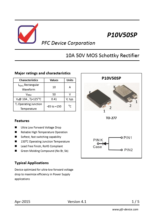
TO-277
1 2
Apr-2015
Version 4.1
1/5
.pfc-device.
Characteristics
1. Characteristics
Maximum Ratings Characteristics
( TA = 25 o C unless otherwise specified )
Parameter DC Blocking Voltage Working Peak Reverse Voltage Peak Repetitive Reverse Voltage Average Rectified Forward Current Per device Peak Forward Surge Current
- 1/2...