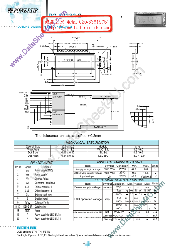
PG12232_B Overview
Key Features
- other Specs not available on catalog is under request
- m o .c U 4 t e e h S a at .D w w w 50oC 70oC 0.04 Vdd=5V 1.0 2.5 120 0.45 V V V V mA mA mA
| Part | PG12232_B |
|---|---|
| Description | LCD_Module |
| Manufacturer | POWERTIP |
| Size | 102.91 KB |
| Part Number | Manufacturer | Description |
|---|---|---|
| PG12232-A | Powertip Technology | LCD |
| PG12232 | Powertip Technology | LCD |
| PG12232-C | Powertip Technology | LCD |
| PG12232-E-33 | Powertip Technology | LCD |
| PG12232-F | Powertip Technology | LCD |