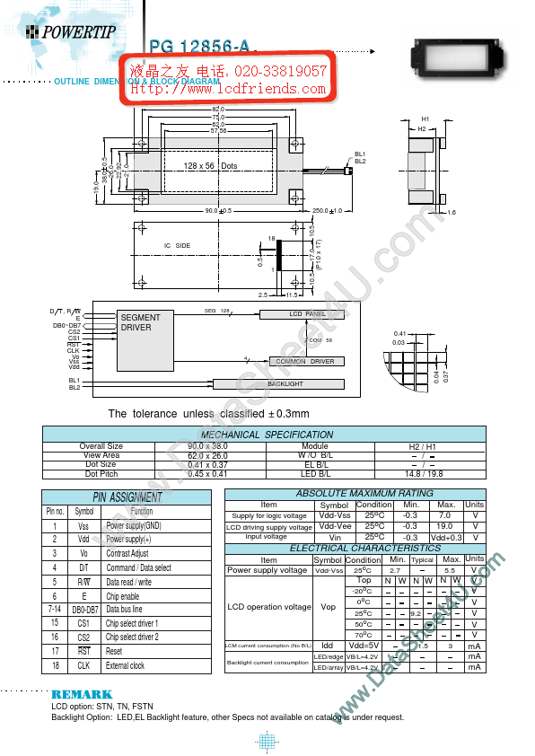
pg12856a Description
Units V 7.0 19.0 V Vdd+0.3 V Item Symbol Condition Min. STN, TN, FSTN Backlight Option:.
pg12856a is LCD_Module manufactured by POWERTIP.
| Part Number | Description |
|---|---|
| pg128128a | LCD_Module |
| PG128128_A | LCD_Module |
| pg12864 | LCD_Module |
| pg12864ak | LCD_Module |
| pg12864ap6 | LCD_Module |
Units V 7.0 19.0 V Vdd+0.3 V Item Symbol Condition Min. STN, TN, FSTN Backlight Option:.