pg12864b
pg12864b is LCD_Module manufactured by POWERTIP.
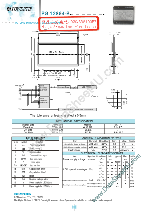
PG 12864-B
OUTLINE DIMENSION & BLOCK DIAGRAM
39.0 0.4 77.2 72.0 66.52 4- 2.5 H1 H2
70.0 0.5 65.0
40.0 50.2
128 x 64 Dots
20 20- 1.0 1.8 PITCH2.54 x 19=48.26 73.0 78.0 0.5 2.5
1 2.5
DB0~DB7 CS1 D /I R/W RST Vss Vdd Vo E CS2
LCD Sesment DRIVER 1
4 mon Driver
64 SEG 64
LCD PANEL
Vout
Voitage Genertor / Temperature pensation
The tolerance unless classified
Overall Size View Area Dot Size Dot Pitch
MECHANICAL SPECIFICATION
PIN ASSIGNMENT
Pin no. 1 2 3 4 5 6 7-14 15 16 17 18 19 20 Symbol Vss Vdd Vo D/I R/W E DB0~DB7 CS1 CS2 RST Vout A K
Function Power supply(GND) Power supply(+) Contrast Adjust mand / data input Data read / write Enable signal...