pg12864h Description
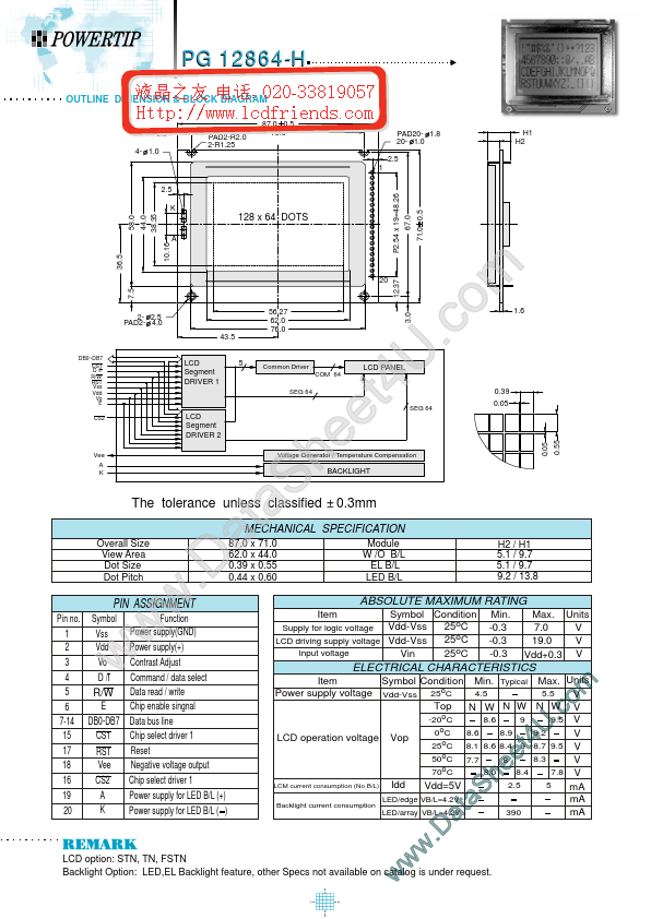
Units V 7.0 19.0 V Vdd+0.3 V Max. Units 5.5 V N W V 9.5 V Item Power supply voltage Symbol Condition Vdd-Vss 25oC 0.05 Min. STN, TN, FSTN Backlight Option:.
pg12864h is LCD_Module manufactured by POWERTIP.
| Manufacturer | Part Number | Description |
|---|---|---|
| PG12864-A | LCD | |
| PG12864-B | LCD | |
| PG12864-D | LCD | |
| PG12864-F | LCD | |
| PG12864-I | LCD |
Units V 7.0 19.0 V Vdd+0.3 V Max. Units 5.5 V N W V 9.5 V Item Power supply voltage Symbol Condition Vdd-Vss 25oC 0.05 Min. STN, TN, FSTN Backlight Option:.