Datasheet Summary
PG 9732-D
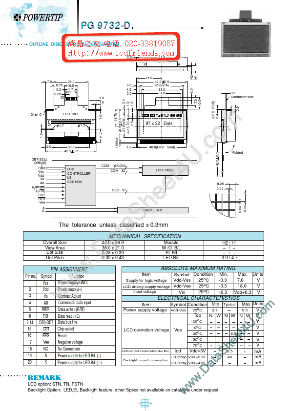
OUTLINE DIMENSION & BLOCK DIAGRAM
0.5 8.5 K 41.0 25.0
21.0 7.0 8.75 0.5 (P0.5 x 19) 0.25 1 20 A 2- 1.0 41 1.5 FPC SIDE K 1.0 28.0 10.5 9.5 3.0 4.5 5.5 3.4 1.0 1.0 3.0 1.0 42.0 0.5 36.0(V/A) 33.0 31.0
H2 H1
0.3 Conductor side 7.0 10.0 (LED PCB) 0.4 0.9 1.0 Folded 27.5
DB7(SCL) DB6(SI) DB0 Vss Vdd Vo Ao
R W(WR)
E(RD) CS1 RES Vee A K
The tolerance unless classified
Overall Size View Area Dot Size Dot Pitch 42.0 x 39.9 36.0 x 21.0 0.28 x 0.39 0.32 x 0.43
PIN ASSIGNMENT
Pin no. 1 2 3 4 5 6 7-14 15 16 17 18 19 20 Symbol Vss Vdd Vo A0 WR RD DB0-DB7 CS1 RES Vee NC A K
Function Power supply(GND) Power supply(+) Contrast Adjust mand / data input Data write / (R/W)...