PJA63P02 Key Features
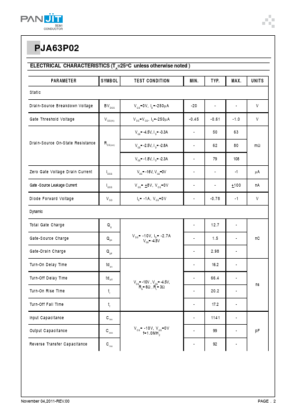
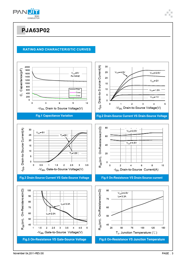
- RDS(ON), VGS@-1.8V,ID@-2.3A<108 mΩ
- RDS(ON), VGS@-4.5V,ID@-3.3A<63 mΩ
- Advanced Trench Process Technology
- High Density Cell Design For Ultra Low On-Resistance
- Specially Designed for DC/DC Converters
- Low Gate Charge
- Lead free in ply with EU RoHS 2002/95/EC directives
- Green molding pound as per IEC61249 Std. . (Halogen Free)
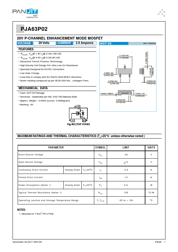
- Case: SOT-23 Package
- Terminals : Solderable per MIL-STD-750,Method 2026