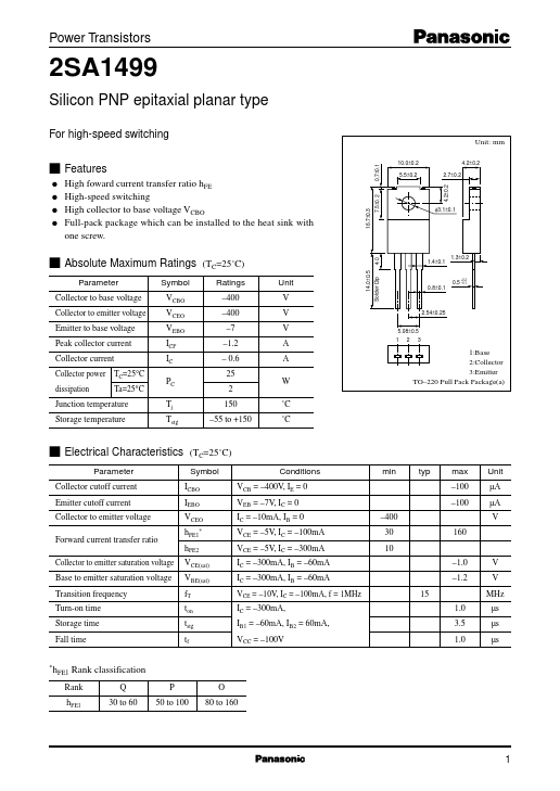
Power Transistors
2SA1499
Silicon PNP epitaxial planar type
For high-speed switching
s Features
q High foward current transfer ratio hFE
q High-speed switching
q High collector to base voltage VCBO
q Full-pack package which can be installed to the heat sink with
one screw.
s Absolute Maximum Ratings (TC=25˚C)
Parameter
Symbol
Ratings
Collector to base voltage
Collector to emitter voltage
Emitter to base voltage
Peak collector current
Collector current
Collector power TC=25°C
dissipation
Ta=25°C
VCBO
VCEO
VEBO
ICP
IC
PC
–400
–400
–7
–1.2
– 0.6
25
2
Junction temperature
Storage temperature
Tj 150
Tstg –55 to +150
Unit
V
V
V
A
A
W
˚C
˚C
10.0±0.2
5.5±0.2
Unit: mm
4.2±0.2
2.7±0.2
φ3.1±0.1
1.3±0.2
1.4±0.1
0.8±0.1
0.5 +0.2
–0.1
2.54±0.25
5.08±0.5
123
1:Base
2:Collector
3:Emitter
TO–220 Full Pack Package(a)
s Electrical Characteristics (TC=25˚C)
Parameter
Symbol
Conditions
min typ max Unit
Collector cutoff current
Emitter cutoff current
ICBO VCB = –400V, IE = 0
IEBO VEB = –7V, IC = 0
–100
–100
µA
µA
Collector to emitter voltage
Forward current transfer ratio
VCEO
hFE1*
hFE2
IC = –10mA, IB = 0
VCE = –5V, IC = –100mA
VCE = –5V, IC = –300mA
–400
30
10
V
160
Collector to emitter saturation voltage VCE(sat)
Base to emitter saturation voltage VBE(sat)
IC = –300mA, IB = –60mA
–1.0 V
–1.2 V
Transition frequency
Turn-on time
Storage time
Fall time
fT VCE = –10V, IC = –100mA, f = 1MHz
ton IC = –300mA,
tstg IB1 = –60mA, IB2 = 60mA,
tf VCC = –100V
15 MHz
1.0 µs
3.5 µs
1.0 µs
*hFE1 Rank classification
Rank
Q
P
hFE1 30 to 60 50 to 100
O
80 to 160
1