C3972
Features q High-speed switching
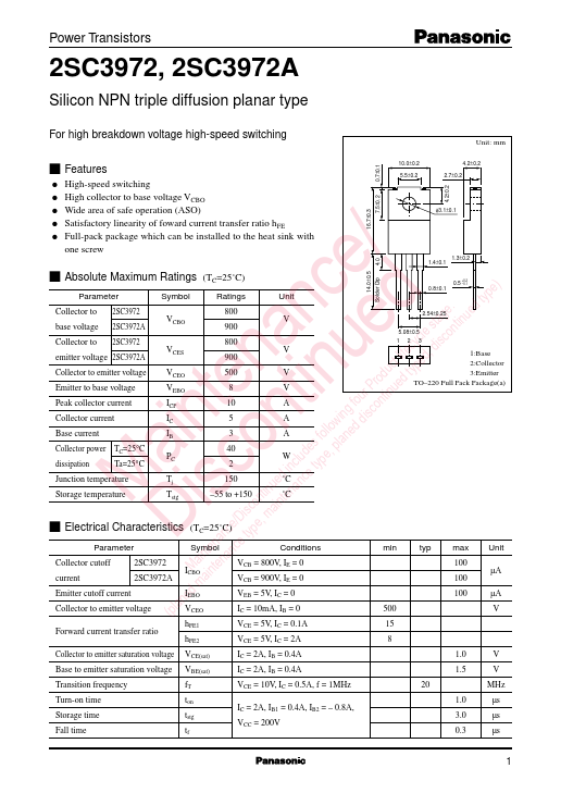
0.7±0.1
10.0±0.2 5.5±0.2
4.2±0.2 2.7±0.2
4.2±0.2
16.7±0.3 7.5±0.2 q High collector to base voltage VCBO q Wide area of safe operation (ASO)
φ3.1±0.1 q Satisfactory linearity of foward current transfer ratio h FE q Full-pack package which can be installed to the heat sink with
/ one screw
1.3±0.2 1.4±0.1 s Absolute Maximum Ratings (TC=25˚C) e pe) Parameter
Symbol
Ratings
Unit
14.0±0.5 Solder Dip 4.0 nc d ge. ed ty Collector to 2SC3972
800 sta tinu base voltage 2SC3972A
VCBO
V a e cycle iscon Collector to 2SC3972
800 life d, d emitter voltage 2SC3972A
VCES
V n u duct type Collector to emitter voltage VCEO
V te tin Pro ued Emitter to base voltage
VEBO
V four ntin Peak collector current
A ing isco Collector current
A in n follow ed d Base current
A es plan Collector power TC=25°C a o includ type, dissipation
Ta=25°C
40 W
2 c ed ce Junction temperature M is ntinu tenan...