C4953 Description
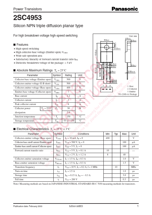
Power Transistors 2SC4953 Silicon NPN triple diffusion planar type For high breakdown voltage high-speed switching 9.9±0.3 Unit: mm 4.6±0.2 2.9±0.2 3.0±0.5.
C4953 Key Features
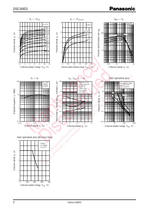
- High-speed switching
- High collector-base voltage (Emitter open) VCBO
- Wide safe operation area
- Satisfactory linearity of forward current transfer ratio hFE
- Dielectric breakdown voltage of the package: > 5 kV