C5517
Features
- High breakdown voltage, and high reliability through the use of a glass passivation layer
- High-speed switching
- Wide area of safe operation (ASO)
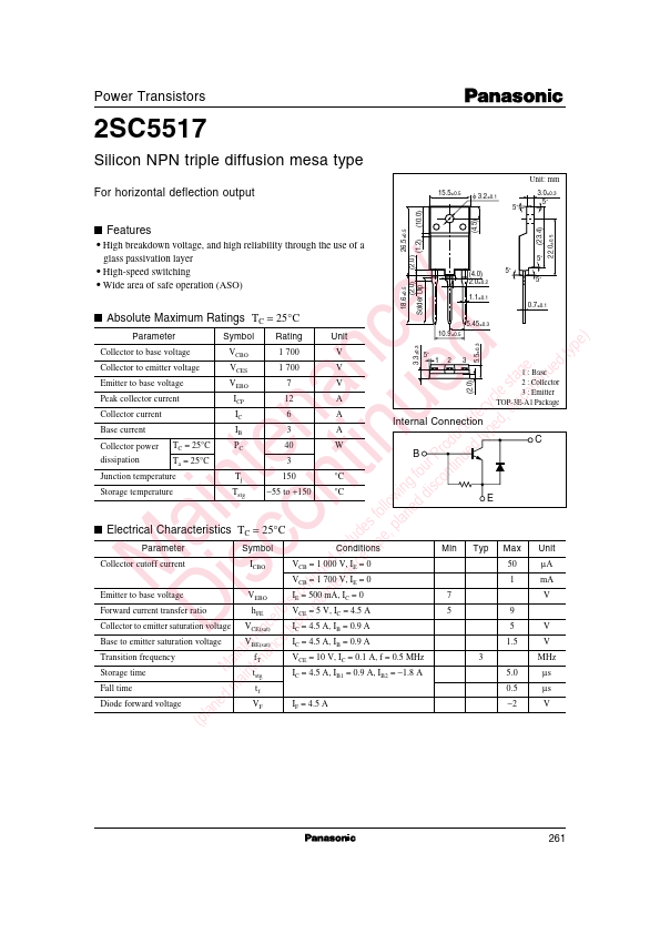
5˚
(4.0)
5˚
2.0±0.2
5˚
/ 1.1±0.1
0.7±0.1
I Absolute Maximum Ratings TC = 25°C
5.45±0.3 e ) Parameter
Symbol Rating
Unit
18.6±0.5 (2.0)
Solder Dip c type Collector to base voltage
VCBO
1 700
3.3±0.3
5.5±0.3 n d ge. ed Collector to emitter voltage
VCES
1 700
(2.0)
V sta tinu Emitter to base voltage
VEBO
V a e cle con Peak collector current
A lifecy , dis Collector current
A n u ct ed Base current
A du typ Collector power TC = 25°C
W te tin Pro ued dissipation
Ta = 25°C
3 four ntin Junction...