AN6551
Key Features
- Phase compensation circuit
- High gain, low noise
- Output short-circuit protection
- Two circuits symmetrically arranged in 9-pin SIL plastic package
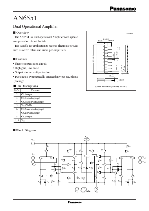
- 3±0.3 6 5 4
- 5±0.25 0.3 - 0.05 + 0.1 2 1
- 0±0.3 s Pin Descriptions Pin No. 2 3 4 5 6 7 8 1, 9 Pin name Ch.1 output Ch.1 inverting input Ch.1 non inverting input VEE (GND) Ch.2 non inverting input Ch.2 inverting input Ch.2 output VCC 9-pin SIL Plastic Package (SIP009-P-0000C) s Block Diagram VCC VCC