Datasheet4U Logo Datasheet4U.com

MN195001 - Single-Chip Fax Engine LSI

Description

Functional Group For Communications Equipment Symbol A0 to 23 MD0 to 7 RD WR R/W CX SCX2 SYNCA HDRES MOD0 to 3 HALT BA IREF0 IREF1 TXLPIN TXOUT RXL IREF2 RXLPIN HPOUT AGCIN AGCOUT SHIN VREFH VREFL PLSD SO to 15 UC0 to 3 IRO1 to 4 U1ST U1RD U1RCK U1SD U1TCK U2ST U2RD U2RCK U2SD U2TCK SH1 to 4 MTA1

Features

  • Digital signal processor (DSP) block.
  • Micro ROM: 4096 × 32 bits.
  • Data RAM: 512 × 16 bits × 2 sets.
  • Machine cycle: 90 ns.
  • Parallel multiplier: 16 bits × 16 bits × → 32 bits.
  • Arithmetic and logic unit (ALU): 32-bit Facsimile peripheral circuit block.
  • Scanner/plotter interface.
  • Two USART channels.
  • Two motor control channels.
  • One thermal head control channel.
  • Programmable chip select Analog circuit block.

📥 Download Datasheet

Datasheet Details

Part number MN195001
Manufacturer Panasonic
File Size 83.57 KB
Description Single-Chip Fax Engine LSI
Datasheet download datasheet MN195001 Datasheet

Full PDF Text Transcription (Reference)

The following content is an automatically extracted verbatim text from the original manufacturer datasheet and is provided for reference purposes only.

View original datasheet text
For Communications Equipment MN195001 Single-Chip Fax Engine LSI Overview 
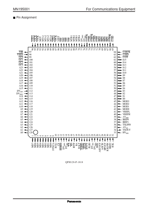
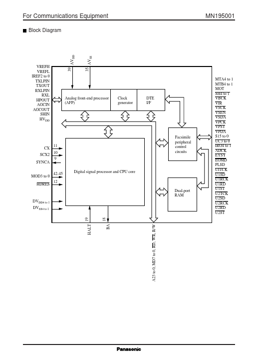
The MN195001 reduces to a single chip CPU functions related to facsimile control, peripheral device control functions, and modem functions. The last include complete fax/modem support for the ITU-T G3 recommandations V.29, V.27ter, and V.21 Channels 1 and 2. The MN195001 consists of the following blocks: digital signal processor (DSP), facsimile peripheral circuits, analog circuits, DTE interface, clock generator, and dualport RAM. Changing the contents of an external ROM tailors the chip for a wide variety of facsimile applications.
Published: |