PE45361
Features
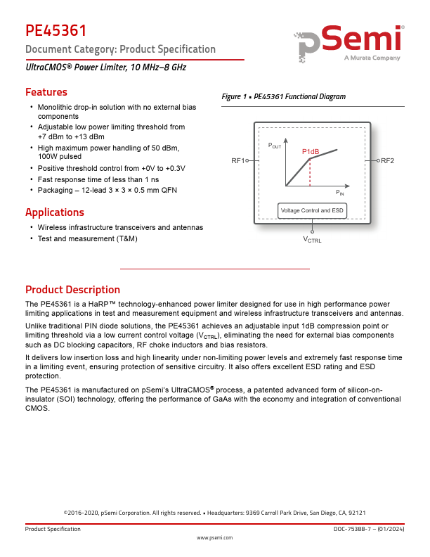
Figure 1
- PE45361 Functional Diagram
- Monolithic drop-in solution with no external bias ponents
- Adjustable low power limiting threshold from +7 d Bm to +13 d Bm
- High maximum power handling of 50 d Bm,
POUT
P1d B
100W pulsed
RF1
RF2
- Positive threshold control from +0V to +0.3V
- Fast response time of less than 1 ns
- Packaging
- 12-lead 3 × 3 × 0.5 mm QFN
Applications
- Wireless infrastructure transceivers and antennas
- Test and measurement (T&M)
Voltage Control and ESD
VCTRL
Product Description
The PE45361 is a Ha RP™ technology-enhanced power limiter designed for use in high performance power limiting applications in test and measurement equipment and wireless infrastructure transceivers and antennas.
Unlike traditional PIN diode solutions, the PE45361 achieves an adjustable input 1d B pression point or limiting threshold via a low current control voltage (VCTRL), eliminating the need for external bias ponents such as DC blocking capacitors, RF choke inductors and bias resistors.
It delivers low insertion loss and high linearity under non-limiting power levels and extremely fast response time in a limiting event, ensuring protection of sensitive circuitry. It also offers excellent ESD rating and ESD protection.
The PE45361 is manufactured on p Semi’s Ultra CMOS® process, a patented advanced form of silicon-oninsulator (SOI) technology, offering the performance of Ga As with the economy and integration of conventional CMOS.
©2016-2020, p Semi Corporation. All rights reserved.
- Headquarters: 9369 Carroll Park Drive, San Diego, CA, 92121
Product Specification
.psemi.
DOC-75388-7
- (01/2024)
PE45361 Ultra CMOS® Power Limiter
Revision History
Table 1
- Revision History
Document Revision
Date
DOC-75388-7
January...