PI6C49X0202 Description
The PI6C49X0202 is a low skew, 1-to-2 LVCMOS/LVTTL High Performance Fanout Buffer. The PI6C49X0202 has a single ended clock input. The single ended clock input accepts LVCMOS or LVTTL input levels.
PI6C49X0202 is 1-To-2 LVCMOS / LVTTL Fanout Buffer manufactured by Pericom Semiconductor.
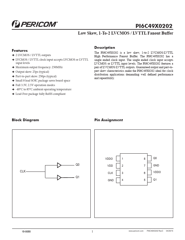
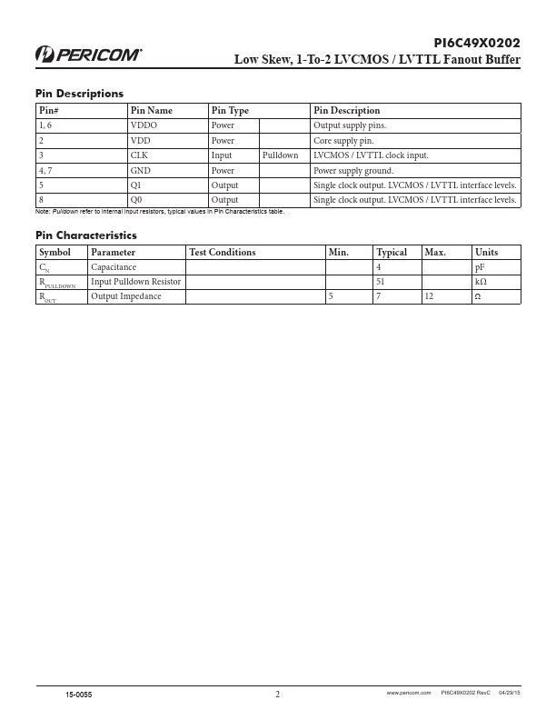
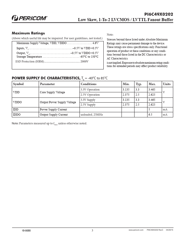
The PI6C49X0202 is a low skew, 1-to-2 LVCMOS/LVTTL High Performance Fanout Buffer. The PI6C49X0202 has a single ended clock input. The single ended clock input accepts LVCMOS or LVTTL input levels.