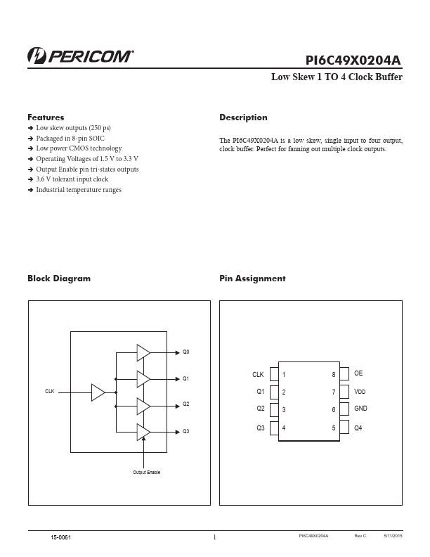
Datasheet4U Logo Datasheet4U.com

PI6C49X0204A - Low Skew 1 TO 4 Clock Buffer

General Description

The PI6C49X0204A is a low skew, single input to four output, clock buffer.

Perfect for fanning out multiple clock outputs.

Key Features

  • ÎÎLow skew outputs (250 ps) ÎÎPackaged in 8-pin SOIC ÎÎLow power CMOS technology ÎÎOperating Voltages of 1.5 V to 3.3 V ÎÎOutput Enable pin tri-states outputs ÎÎ3.6 V tolerant input clock ÎÎIndustrial temperature ranges PI6C49X0204A Low Skew 1 TO 4 Clock Buffer.

📥 Download Datasheet

Full PDF Text Transcription for PI6C49X0204A (Reference)

Note: Below is a high-fidelity text extraction (approx. 800 characters) for PI6C49X0204A. For precise diagrams, and layout, please refer to the original PDF.

Features ÎÎLow skew outputs (250 ps) ÎÎPackaged in 8-pin SOIC ÎÎLow power CMOS technology ÎÎOperating Voltages of 1.5 V to 3.3 V ÎÎOutput Enable pin tri-states outputs ÎÎ...

View more extracted text
g Voltages of 1.5 V to 3.3 V ÎÎOutput Enable pin tri-states outputs ÎÎ3.6 V tolerant input clock ÎÎIndustrial temperature ranges PI6C49X0204A Low Skew 1 TO 4 Clock Buffer Description The PI6C49X0204A is a low skew, single input to four output, clock buffer. Perfect for fanning out multiple clock outputs. Block Diagram Pin Assignment CLK 15-0061 Q0 Q1 Q2 Q3 Output Enable CLK 1 Q1 2 Q2 3 Q3 4 8 OE 7 VDD 6 GND 5 Q4 1 PI6C49X0204A Rev C 5/11/2015 PI6C49X0204A Low Skew 1 TO 4 Clock Buffer Pin Descriptions Pin# 1 2 3 4 5 6 7 Pin Name CLK Q1 Q2 Q3 Q4 GND VDD 8 OE Pin Type Input Output Output Output Output Power Power Input Pin De