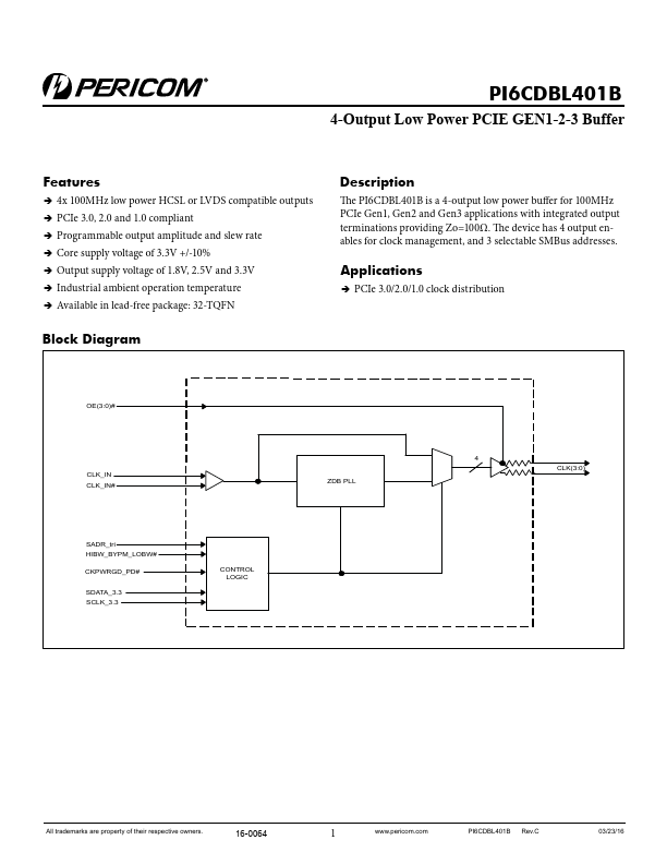
Datasheet4U Logo Datasheet4U.com

PI6CDBL401B - 4-Output Low Power PCIE GEN1-2-3 Buffer

General Description

The PI6CDBL401B is a 4-output low power buffer for 100MHz PCIe Gen1, Gen2 and Gen3 applications with integrated output terminations providing Zo=100Ω.

The device has 4 output enables for clock management, and 3 selectable SMBus addresses.

Key Features

  • ÎÎ4x 100MHz low power HCSL or LVDS compatible outputs ÎÎPCIe 3.0, 2.0 and 1.0 compliant ÎÎProgrammable output amplitude and slew rate ÎÎCore supply voltage of 3.3V +/-10% ÎÎOutput supply voltage of 1.8V, 2.5V and 3.3V ÎÎIndustrial ambient operation temperature ÎÎAvailable in lead-free package: 32-TQFN Block Diagram.

📥 Download Datasheet

Full PDF Text Transcription for PI6CDBL401B (Reference)

Note: Below is a high-fidelity text extraction (approx. 800 characters) for PI6CDBL401B. For precise diagrams, and layout, please refer to the original PDF.

PI6CDBL401B 4-Output Low Power PCIE GEN1-2-3 Buffer Features ÎÎ4x 100MHz low power HCSL or LVDS compatible outputs ÎÎPCIe 3.0, 2.0 and 1.0 compliant ÎÎProgrammable output...

View more extracted text
atible outputs ÎÎPCIe 3.0, 2.0 and 1.0 compliant ÎÎProgrammable output amplitude and slew rate ÎÎCore supply voltage of 3.3V +/-10% ÎÎOutput supply voltage of 1.8V, 2.5V and 3.3V ÎÎIndustrial ambient operation temperature ÎÎAvailable in lead-free package: 32-TQFN Block Diagram Description The PI6CDBL401B is a 4-output low power buffer for 100MHz PCIe Gen1, Gen2 and Gen3 applications with integrated output terminations providing Zo=100Ω. The device has 4 output enables for clock management, and 3 selectable SMBus addresses. Applications ÎÎPCIe 3.0/2.0/1.0 clock distribution OE(3:0)# CLK_IN CLK_IN# SADR_tri HIBW_BYPM_LOBW# C