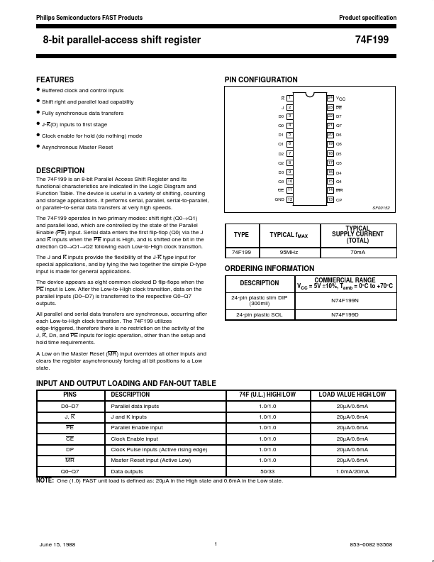
74F199
FEATURES
- Buffered clock and control inputs
- Shift right and parallel load capability
- Fully synchronous data transfers
- J-K(D) inputs to first stage
- Clock enable for hold (do nothing) mode
- Asynchronous Master Reset
DESCRIPTION
The 74F199 is an 8-bit Parallel Access Shift Register and its functional characteristics are indicated in the Logic Diagram and Function Table. The device is useful in a variety of shifting, counting and storage applications. It performs serial, parallel, serial-to-parallel, or parallel- to-serial data transfers at very high speeds. The 74F199 operates in two primary modes: shift right (Q0→Q1) and parallel load, which are controlled by the state of the Parallel Enable (PE) input. Serial data enters the first flip-flop (Q0) via the J and K inputs when the PE input is High, and is shifted one bit in the direction Q0→Q1→Q2 following each Low-to-High clock transition. The J and K inputs provide the flexibility of the J-K type input for special applications,...