Datasheet Summary
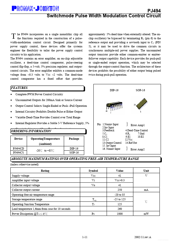
PJ494 Switchmode Pulse Width Modulation Control Circuit he PJ494 incorporates on a single monolithic chip all the functions required in the construction of a pulsewidth-modulation control circuit. Designed primarily for power supply control, these devices offer the systems engineer the flexibility to tailor the power supply control circuitry to his application. The PJ494 contains an error amplifier, an on-chip adjustable oscillator, a deed-time control parator, pulse-steering control flip-flop, a 5-volt, 5% precision regulator, and outputcontrol circuits. The error amplifier exhibits a mon-mode voltage from
- 0.3 volts to Vcc
- 2 volts. The dead-time control parator has a fixed...