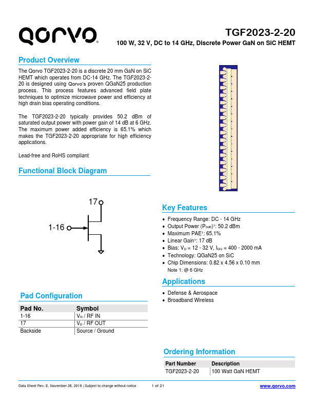
TGF2023-2-20
® 100 W, 32 V, DC to 14 GHz, Discrete Power GaN on SiC HEMT
Absolute Maximum Ratings
Recommended Operating Conditions
Parameter
Rating
Drain to Gate Voltage (VDG)
Gate Voltage Range (VG)
100 V
−7 to +2 V
Drain Current (ID)
Gate Current (IG)
20 A
−20 to 56 mA
Power Dissipation, CW (PD)
See graph on pg.4.
CW Input Power (PIN)
Storage Temperature
+43 dBm
−65 to 150°C
Exceeding any one or a combination of the Absolute Maximum Rating
conditions may cause permanent damage to the device. Extended
application of Absolute Maximum Rating conditions to the device may
reduce device reliability.
Parameter
Min Typ Max Units
Drain Voltage Range (VD)
–
Drain Quiescent Current (IDQ) –
+28
1000
–
–
V
mA
Gate Voltage, VG1
−3.7 −2.8 −2.3 V
Gate Leakage: VD = +10 V,
VG = −3.7 V
−20
–
– mA
Electrical specifications are measured at specified test conditions.
Specifications are not guaranteed over all recommended operating
conditions.
Note:
1. To be adjusted to desired IDQ
RF Characterization – Model Optimum Power Tune
Test conditions unless otherwise noted: T = 25°C, Pulse (10% Duty Cycle, 100 µs Width).
Parameter
Typical Value
Frequency (F)
36
8 10
Drain Voltage (VD)
28 28 28
28
28
28 28 28
Bias Current (IDQ)
400 1000 400
1000
400
1000
400 1000
Output P3dB (P3dB)
50.3 50.2 50.2
50.2
50.2
50.1 50.2 50.2
PAE @ P3dB (PAE3dB)
62.4 61.7 58.7
58.6
56.1
56
53 53.3
Gain @ P3dB (G3dB)
Parallel Resistance (1) (Rp)
Parallel Capacitance (1) (Cp)
Load Reflection Coefficient (2)
(ΓL)
19.1
64.4
0.264
19.9
64.8
0.255
13.2
59.7
0.291
0.20∠131° 0.20∠131° 0.38∠132°
14
59.2
0.295
0.38∠132°
10.7
54.8
0.317
0.49∠137°
11.5
54.4
0.315
9.0
49.6
0.326
9.6
49.2
0.324
0.49∠138° 0.57∠143° 0.56∠143°
Notes:
1. Large signal equivalent output network (normalized).
2. Characteristic Impedance (Zo) = 4 Ω.
Units
GHz
V
mA
dBm
%
dB
Ω∙mm
pF/mm
--
RF Characterization – Model Optimum Efficiency Tune
Test conditions unless otherwise noted: T = 25°C, Pulse (10% Duty Cycle, 100 µs Width).
Parameter
Typical Value
Frequency (F)
36
8
10
Drain Voltage (VD)
28 28 28
28
28
28 28 28
Bias Current (IDQ)
400 1000 400
Output P3dB (P3dB)
48.5 48.7 48.8
PAE @ P3dB (PAE3dB)
69.5 68.5
66
Gain @ P3dB (G3dB)
21.1 21.7 14.7
Parallel Resistance (1) (Rp)
126 123 110
Parallel Capacitance (1) (Cp)
Load Reflection Coefficient (2)
(ΓL)
0.392 0.385 0.388
0.40∠78° 0.39∠78° 0.58∠111°
Notes:
1.
2.
Large signal equivalent output network (normalized).
Characteristic Impedance (Zo) = 4 Ω.
1000
48.9
65.1
15.2
103
0.387
0.56∠112°
400
49.0
62.2
11.8
94.9
0.379
0.64∠124°
1000
49.1
61.8
12.5
90.3
0.379
400
49.2
58.4
10.1
81.6
0.373
1000
49.1
58.4
10.6
80.5
0.378
0.63∠125° 0.69∠133° 0.69∠133°
Units
GHz
V
mA
dBm
%
dB
Ω∙mm
pF/mm
--
Data Sheet Rev. E, November 26, 2019 | Subject to change without notice
2 of 21
www.qorvo.com