Datasheet4U Logo Datasheet4U.com

RCR1540ESJ - P-Channel Enhancement Mode Field Effect Transistor

Datasheet Details

Part number RCR1540ESJ
Manufacturer RCR
File Size 694.66 KB
Description P-Channel Enhancement Mode Field Effect Transistor
Datasheet download datasheet RCR1540ESJ Datasheet

General Description

The RCR1540ESJ uses advanced trench technology to provide excellent RDS(ON), low gate charge and operation with gate voltages as low as 1.8V.

This device is suitable for use as a load switch or in PWM applications.

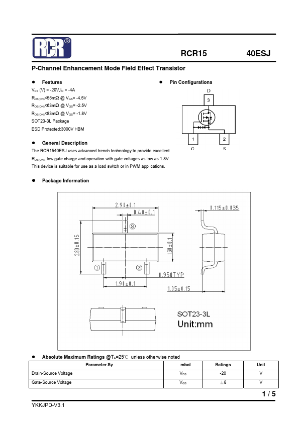
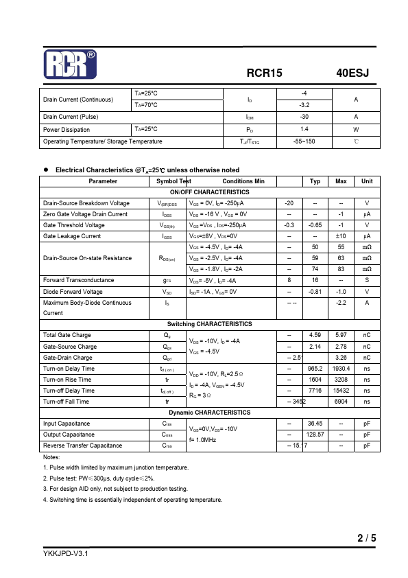
z Package Information z Absolute Maximum Ratings @TA=25℃ unless otherwise noted Parameter Sy mbol VDS VGS Ratings -20 ±8 Unit V V Drain-Source Voltage Gate-Source Voltage 1/5 YKKJPD-V3.1 http://www.Datasheet4U.com ® RCR15 Drain Current (Continuous) Drain Current (Pulse) Power Dissipation TA=25°C TA=25°C TA=70°C ID IDM PD TJ//TSTG -4 -3.2 -30 1.4 -55~150 40ESJ A A W ℃ Operating Temperature/ Storage Temperature z Electrical Characteristics @TA=25℃ unless otherwise noted Parameter Symbol Test Conditions Min Typ Max Unit ON/OFF CHARACTERISTICS Drain-Source Breakdown Voltage Zero Gate Voltage Drain Current Gate Threshold Voltage Gate Leakage Current V(BR)DSS IDSS VGS(th) IGSS VGS = 0V, ID= -250μA VDS = -16 V , VGS = 0V VGS =VDS , IDS=-250μA -20 --0.3 ----8 --- ----0.65 -50 59 74 16 -0.81 --1 -1 ±10 55 63 83 --1.0 -2.2 V μA V μA mΩ mΩ mΩ S V A VGS=±8V , VDS=0V VGS = -4.5V , ID= -4A VGS = -2.5V , ID= -4A VGS = -1.8V , ID= -2A Drain-Source On-state Resistance RDS(on) Forward Transconductance Diode Forward Voltage Maximum Body-Diode Continuous Current gFS VSD IS VDS= -5V , ID= -4A ISD= -1A , VGS= 0V Switching CHARACTERISTICS Total Gate Charge Gate-Source Charge Gate-Drain Charge Turn-on Delay Time Turn-on Rise Time Turn-off Delay Time Turn-off Fall Time Qg Qgs Qgd td ( on ) tr td( off ) tf VDS = -10V, ID = -4A VGS = -4.5V ---- 2.51 ----- 3452 4.59 2.14 5.97 2.78 3.26 nC nC nC ns ns ns ns VDD = -10V, RL=2.5Ω ID = -4A, VGEN = -4.5V RG = 3Ω 965.2 1604 7716 1930.4 3208 15432 6904

Overview

® RCR15 P-Channel Enhancement Mode Field Effect Transistor z.

Key Features

  • z Pin Configurations 40ESJ VDS (V) = -20V,ID = -4A RDS(ON).