BDJ2FD0WFP2-E2
Overview
The BDxxFD0 series are low-saturation regulators. The series’ output voltages are Variable, and fixed type.
- Output current capability: 2A
- Output voltage: Variable, Fixed (1.5V / 1.8V / 2.5V / 3.0V / 3.3V / 5.0V / 8.0V / 9.0V / 12V / 15V / 16V)
- ±1% (±1.5%:BD15/18/25FD0W) High output voltage accuracy (Ta=25°C)
- Low saturation with PDMOS output
- Built-in over-current protection circuit that prevents the destruction of the IC due to output short circuits
- Built-in thermal Shutdown circuit for protecting the IC from thermal damage due to overloading
- Low ESR Capacitor
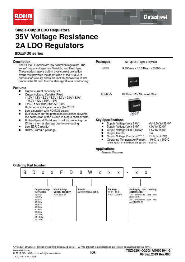
- HRP5/TO263-5 package Packages HRP5 W(Typ) x D(Typ) x H(Max) 9.395mm x 10.540mm x 2.005mm TO263-5
- 16mm×15.10mm×4.70mm Key Specifications
- Supply Voltage(Vo ≥ 3.0V): Vo+1.0V to 32.0V