Datasheet Summary
USB Type-C Power Delivery Controller
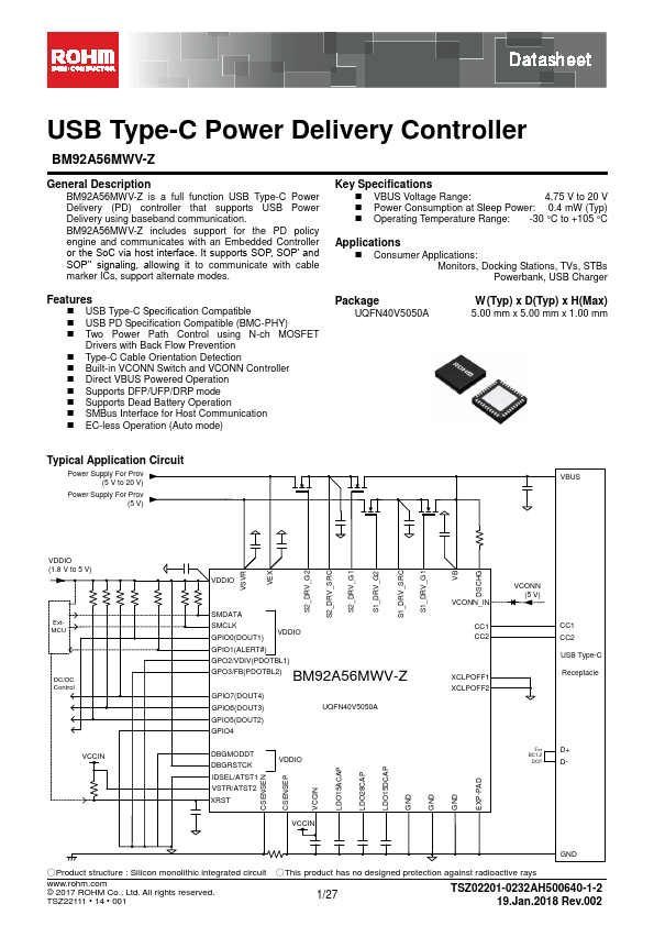
General Description
BM92A56MWV-Z is a full function USB Type-C Power
Delivery (PD) controller that supports USB Power
Delivery using baseband munication.
BM92A56MWV-Z includes support for the PD policy engine and municates with an Embedded Controller or the SoC via host interface. It supports SOP, SOP’ and SOP’’ signaling, allowing it to municate with cable marker ICs, support alternate modes.
Key Specifications
- VBUS Voltage Range:
4.75 V to 20 V
- Power Consumption at Sleep Power: 0.4 mW (Typ)
- Operating Temperature Range: -30 °C to +105 °C
Applications
- Consumer Applications:
Monitors, Docking Stations,...