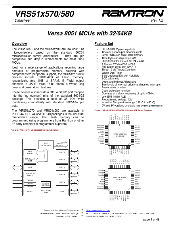
Description
for QFP-44
T ABLE 1: PIN DESCRIPTIONS FOR QFP-44/
QFP - 44
QFP - 44 Function
Name
I/O
Function
Name
I/O
24 25 26 27 28 29 30 31 32 33 34 35 36 37 38 39 40 41 42 43
1 2 3 4 5 6 7 8 9 10 11 12 13 14 15 16 17 18 19 20 21 22 23
P0.4/AD4
P0.5/AD5
P0.6/AD6
P0.7/AD7
#PSEN P2.7/A15
P2.6/A14
P0.3/AD3 P0.2/AD2 P0.1/AD1 P0.0/AD0 VDD P4.2 T2/P1.0 T2EX/P1.1 P1.2 PWM0/P1.3 PWM1/P1.4
34
33
23 22
P2.5/A13
PWM2 P1.5 PWM3 P1.6 PWM4 P1.7 RES RXD P3.0 P4.3 TXD P3.1 #INT0 P3.2 #INT1 P3.3 T0 P3.
Features
- These devices also include a fifth, 4-bit, I/O port mapped into the “no connect” pins of the standard 8051/52 package. This provides a total of 36 I/Os while maintaining compatibility with standard 80C51/52 pin outs. The VRS51x570 and VRS51x580 are available in PLCC-44, QFP-44 and DIP-40 packages in the Industrial temperature range. The Flash memory can be programmed using programmers from Ramtron or other 3rd party commercial programmer suppliers. FIGURE 1: VRS51X570 / VRS51X580.