VRS51L570
Overview
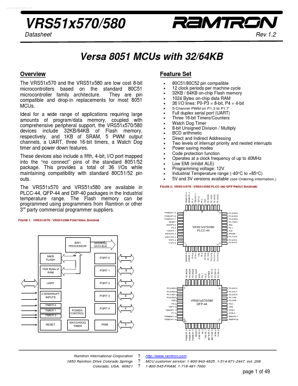
- 80C51/80C52 pin compatible 12 clock periods per machine cycle 32KB / 64KB on-chip Flash memory 1024 Bytes on-chip data RAM 36 I/O lines: P0-P3 = 8-bit, P4 = 4-bit 5-Channel PWM on P1.3 to P1.7 Full duplex serial port (UART) Three 16-bit Timers/Counters Watch Dog Timer 8-bit Unsigned Division / Multiply BCD arithmetic Direct and Indirect Addressing Two levels of interrupt priority and nested interrupts Power saving modes Code protection function Operates at a clock frequency of up to 40MHz Low EMI (inhibit ALE) Programming voltage: 12V Industrial Temperature range (-40°C to +85°C) 5V and 3V versions available (see Ordering information.) FIGURE 2: VRS51X570 / VRS51X580 PLCC AND QFP PINOUT DIAGRAMS PWM0/P1.3 PWM1/P1.4 P1.2 T2EX/P1.1 P0.0/AD0 P0.2/AD2 PWM2/P1.5 PWM3/P