5P1105 Description
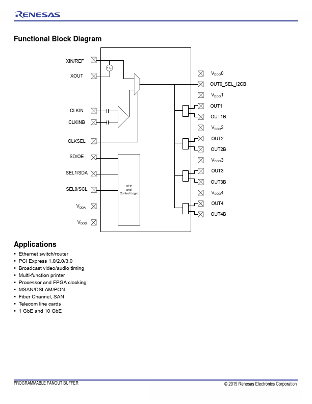
The 5P1105 is a programmable fanout buffer intended for high performance consumer, networking, industrial, puting, and data-munications applications. Configurations may be stored in on-chip One-Time Programmable (OTP) memory or changed using I2C interface. The outputs are generated from a single reference clock.
5P1105 Key Features
- Up to four high performance universal differential output
- Low RMS additive phase jitter: 0.2ps
- Four banks of internal non-volatile in-system
- I2C serial programming interface
- One additional LVCMOS output clock
- Four universal output pairs
- Each configurable as one differential output pair or two LVCMOS outputs
- I/O Standards
- Single-ended I/Os: 1.8V to 3.3V LVCMOS
- Differential I/Os
5P1105 Applications
- Up to four high performance universal differential output