5PB1104PGGI
5PB1104PGGI is 1.8V to 3.3V High-Performance LVCMOS Clock Buffer manufactured by Renesas.
- Part of the 5PB1102PGG comparator family.
- Part of the 5PB1102PGG comparator family.
1.8V to 3.3V High-Performance LVCMOS Clock Buffer Family
5PB11xx Datasheet
Description
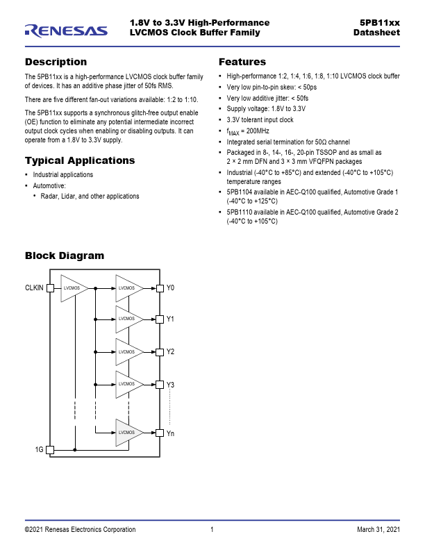
The 5PB11xx is a high-performance LVCMOS clock buffer family of devices. It has an additive phase jitter of 50fs RMS.
There are five different fan-out variations available: 1:2 to 1:10.
The 5PB11xx supports a synchronous glitch-free output enable (OE) function to eliminate any potential intermediate incorrect output clock cycles when enabling or disabling outputs. It can operate from a 1.8V to 3.3V supply.
Typical Applications
- Industrial applications
- Automotive:
- Radar, Lidar, and other applications
Features
- High-performance 1:2, 1:4, 1:6, 1:8, 1:10 LVCMOS clock buffer
- Very low pin-to-pin...