5PB1213
5PB1213 is TCXO/LVCMOS Clock Buffer manufactured by Renesas.
- Part of the 5PB1203 comparator family.
- Part of the 5PB1203 comparator family.
Description
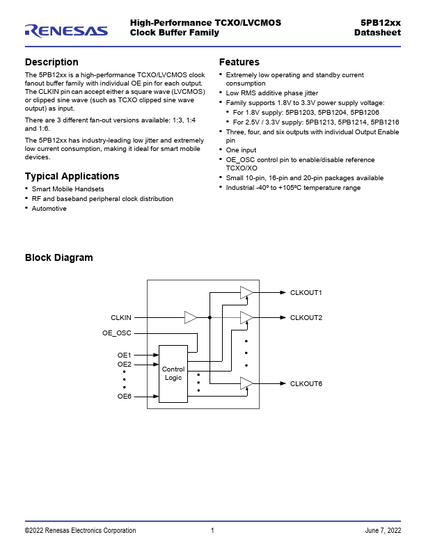
The 5PB12xx is a high-performance TCXO/LVCMOS clock fanout buffer family with individual OE pin for each output. The CLKIN pin can accept either a square wave (LVCMOS) or clipped sine wave (such as TCXO clipped sine wave output) as input.
There are 3 different fan-out versions available: 1:3, 1:4 and 1:6.
The 5PB12xx has industry-leading low jitter and extremely low current consumption, making it ideal for smart mobile devices.
Typical Applications
- Smart Mobile Handsets
- RF and baseband peripheral clock distribution
- Automotive
Features
- Extremely low operating and standby current consumption
- Low RMS additive phase jitter
- Family supports 1.8V to 3.3V power supply voltage:
- For 1.8V supply: 5PB1203, 5PB1204, 5PB1206
- For 2.5V / 3.3V supply: 5PB1213, 5PB1214, 5PB1216
- Three, four, and six outputs with individual Output Enable pin
- One input
- OE_OSC control pin to enable/disable reference
TCXO/XO
- Small 10-pin, 16-pin and 20-pin packages available
- Industrial -40º to +105ºC temperature range
Block Diagram
CLKIN OE_OSC
OE1 OE2
OE6
Control Logic
CLKOUT1 CLKOUT2
CLKOUT6
©2022 Renesas Electronics Corporation
June 7, 2022
Pin Assignments
5PB12xx Datasheet
OE1 CLKIN GND CLKOUT1
CLKIN OE1 GND CLKOUT1 CLKOUT2
CLKIN
E_OSC
OE3...