Datasheet Summary
High-Performance TCXO/LVCMOS Clock Buffer Family
5PB12xx Datasheet
Description
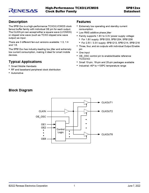
The 5PB12xx is a high-performance TCXO/LVCMOS clock fanout buffer family with individual OE pin for each output. The CLKIN pin can accept either a square wave (LVCMOS) or clipped sine wave (such as TCXO clipped sine wave output) as input.
There are 3 different fan-out versions available: 1:3, 1:4 and 1:6.
The 5PB12xx has industry-leading low jitter and extremely low current consumption, making it ideal for smart mobile devices.
Typical Applications
- Smart Mobile Handsets
- RF and baseband peripheral clock distribution
- Automotive
Features
- Extremely low operating and standby current consumption
- Low RMS...