8413S12B
8413S12B is HCSL/ LVCMOS Clock Generator manufactured by Renesas.
HCSL/ LVCMOS Clock Generator
General Description
The 8413S12B is a PLL-based clock generator. This high performance device is optimized to generate the processor core reference clock, the PCI-Express, s RIO, XAUI, Ser Des reference clocks and the clocks for both the Gigabit Ethernet MAC and PHY. The clock generator offers ultra low-jitter, low-skew clock outputs. The output frequencies are generated from a 25MHz external input source or an external 25MHz parallel resonant crystal. The industrial temperature range of the 8413S12B supports telemunication, networking, and storage requirements.
Applications
- CPE Gateway Design
- Home Media Servers
- 802.11n AP or Gateway
- Soho Secure Gateway
- Soho SME Gateway
- Wireless Soho and SME VPN Solutions
- Wired and Wireless Network Security
- Web Servers and Exchange Servers
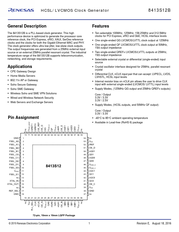
Pin Assignment
Features
- Ten selectable 100MHz, 125MHz, 156.25MHz and 312.5MHz clocks for PCI Express, s RIO and Gb E, HCSL interface levels
- One single-ended QG LVCMOS/LVTTL clock output at 125MHz
- One single-ended QF LVCMOS/LVTTL clock output at 50MHz,
15 output impedance
- Two single-ended QREFx LVCMOS/LVTTL outputs at 25MHz,
15 output impedance
- Selectable external crystal or differential (single-ended) input source
- Crystal oscillator interface designed for 25MHz, parallel resonant crystal
- Differential CLK, n CLK input pair that can accept: LVPECL, LVDS,
LVHSTL, HCSL input levels
- Internal resistor bias on n CLK pin allows the user to drive CLK input with external single-ended (LVCMOS/ LVTTL) input levels
- Supply Modes, (125MHz QG output and 25MHz QREFx outputs):
Core / Output 3.3V / 3.3V 3.3V / 2.5V
- Supply Modes, (HCSL outputs, and 50MHz QF output):
Core / Output 3.3V / 3.3V
- -40°C to 85°C ambient operating...