853S058
853S058 is LVPECL/ECL Clock Multiplexer manufactured by Renesas.
8:1 Differential-to-3.3V or 2.5V LVPECL/ECL Clock Multiplexer
DATA SHEET
General Description
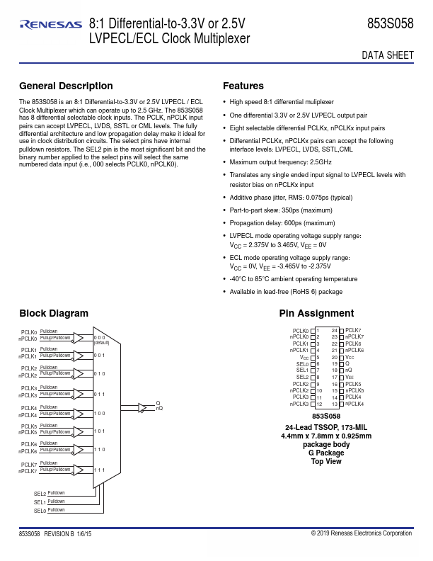
The 853S058 is an 8:1 Differential-to-3.3V or 2.5V LVPECL / ECL Clock Multiplexer which can operate up to 2.5 GHz. The 853S058 has 8 differential selectable clock inputs. The PCLK, n PCLK input pairs can accept LVPECL, LVDS, SSTL or CML levels. The fully differential architecture and low propagation delay make it ideal for use in clock distribution circuits. The select pins have internal pulldown resistors. The SEL2 pin is the most significant bit and the binary number applied to the select pins will select the same numbered data input (i.e., 000 selects PCLK0, n PCLK0).
Block Diagram
PCLK0 Pulldown n PCLK0 Pullup/Pulldown
PCLK1 Pulldown n PCLK1 Pullup/Pulldown
PCLK2 Pulldown n PCLK2 Pullup/Pulldown
PCLK3 Pulldown n PCLK3 Pullup/Pulldown
PCLK4 Pulldown n PCLK4 Pullup/Pulldown
PCLK5 Pulldown n PCLK5 Pullup/Pulldown
PCLK6 Pulldown n PCLK6 Pullup/Pulldown
PCLK7 Pulldown n PCLK7 Pullup/Pulldown
000 (default) 001 010
100 101 110
Q n Q
Features
- High speed 8:1 differential muliplexer
- One differential 3.3V or 2.5V LVPECL output pair
- Eight selectable differential PCLKx, n PCLKx input pairs
- Differential PCLKx, n PCLKx pairs can accept the following interface levels: LVPECL, LVDS, SSTL,CML
- Maximum output frequency: 2.5GHz
- Translates any single ended input signal to LVPECL levels with resistor bias on n PCLKx input
- Additive phase jitter, RMS: 0.075ps (typical)
- Part-to-part skew: 350ps (maximum)
- Propagation delay: 600ps (maximum)
- LVPECL mode operating voltage supply range:
VCC = 2.375V to 3.465V, VEE = 0V
- ECL mode operating voltage supply range:
VCC = 0V, VEE = -3.465V to...