9DBL0452
Overview
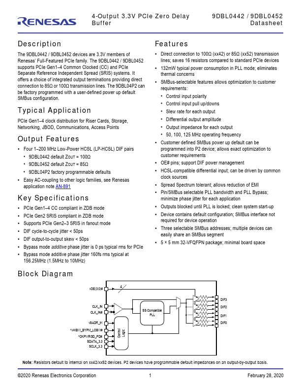
The 9DBL0442 / 9DBL0452 devices are 3.3V members of Renesas’ Full-Featured PCIe family. The 9DBL0442 / 9DBL0452 supports PCIe Gen1-4 Common Clocked (CC) and PCIe Separate Reference Independent Spread (SRIS) systems.
- 9DBL0442 default ZOUT = 100Ω
- 9DBL0452 default ZOUT = 85Ω
- 9DBL04P2 factory programmable defaults; Easy AC-coupling to other logic families, see Renesas application note AN-891 Key Specifications; PCIe Gen1-4 CC compliant in ZDB mode; PCIe Gen2 SRIS compliant in ZDB mode; Supports PCIe Gen2-3 SRIS in fanout mode; DIF cycle-to-cycle jitter < 50ps; DIF output-to-output skew < 50ps; Bypass mode additive phase jitter is 0 ps typical rms for PCIe; Bypass mode additive phase jitter 160fs rms typical at
- 25MHz (1.5MHz to 10MHz) Features; Direct connection to 100Ω (xx42) or 85Ω (xx52) transmission lines; saves 16 resistors compared to standard PCIe devices; 132mW typical power consumption in PLL mode; eliminates thermal concerns; SMBus-selectable features allows optimization to customer requirements:
- Control input polarity
- Control input pull up/downs
- Slew rate for each output
- Differential output amplitude
- Output impedance for each output
- 50, 100, 125 MHz operating frequency; Customer defined SMBus power up default can be programmed into P2 device; allows exact optimization to customer requirements; OE# pins; support DIF power management; HCSL-compatible differential input; can be