9DBV0231
9DBV0231 is 2-Output 1.8V PCIe Zero-Delay/Fanout Clock Buffer manufactured by Renesas.
2-Output 1.8V PCIe Zero-Delay/Fanout Clock Buffer with Zo = 33Ohms
Description
The 9DBV0231 is a member of Renesas’ 1.8V Very-Low-Power (VLP) PCIe family. The device has 2 output enables for clock management.
Remended Application
1.8V PCIe Gen1- 5 Zero-Delay/Fan-out Buffer (ZDB/FOB)
Output Features
- Two 1- 200MHz Low-Power (LP) HCSL DIF pairs
Key Specifications
- DIF cycle-to-cycle jitter < 50ps
- DIF output-to-output skew < 50ps
- PCIe Gen5 CC additive phase jitter < 40fs RMS
- 12kHz- 20MHz additive phase jitter = 156fs RMS at
156.25MHz (typical)
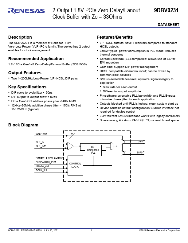
Block Diagram
Features
/Benefits
- LP-HCSL outputs; save 4 resistors pared to standard
HCSL outputs
- 35mW typical...